System integration for nanophotonic systems
- Contact:
- Project Group: System integration - system-, process- and equipment development
- Funding:
HGF, BMBF
- Partner: IMT/KIT, IPQ/KIT, APH/KIT, Partner BMBF-Projekt PHOIBOS
- Startdate:
2014
Program: Science and Technology of Nanosystems (STN) - Topic 3 Optics Photonics - Subtopic Teratronics
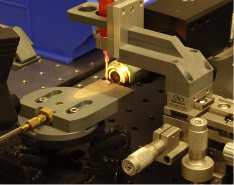
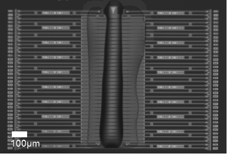
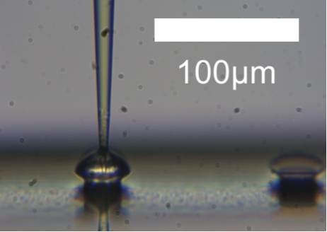
Systems based on nanophotonic technologies enable promising, new applications in different fields. In addition to sensor applications, solutions in the data communication field are hereby also worth mentioning. Devices that are based on photonics make it possible to develop communication modules that have very high data rates at reduced power consumption. The high integration of photonic devices is another defining characteristic of this technology. Current development trends are characterized by solutions that make it increasingly easier to integrate the functions associated with the transmitted signal (modulation, amplification, filtering, distribution) on a chip. One essential feature is the combination of sub-systems that are developed using different technologies on different chips together into one system. These could be photonic structures from, e.g., light sources (e.g., laser diodes) based on III-V compound semi-conductors coupled with silicon photonic chips coupled to an optical fiber. An important technique for constructing such multi-chip modules is the optical connection technology that uses photonic wire bonds. These are fabricated using two-photon polymerization. The technology is being developed at the KIT Institute for Photonics and Quantum Electronics IPQ and the Institute for Micro-structure Technology IMT. The research on nanophotonic systems integration at the IAI aims to develop processes and process modules for the construction of such multi-chip modules (Figure 1). Besides the handling of individual components, this also entails high-precision and selective dispensing of process fluids on optical chips as well as the design and realization of complete process chains with the required new equipment technology or appropriate adaptation of the standard equipment available on the market. The micro-dispensing processes for the realization of efficient and low-loss chip-to-chip connections (Figure 2) are also used in selective functionalization of bio-photonic sensors based on goblet resonators and other bio-photonic applications (Figure 3).