
System integration for printed materials and systems
- Contact:
- Project Group: System integration - system-, process- and equipment development
- Funding:
HGF POF III
- Partner: IAM, IMT, INT, IPE, LTI
- Startdate:
2015
Functional printing can be used to fabricate complex, miniaturized systems on flexible polymer substrates. Multi-layered structures allow for diverse applications such as Internet of Things (IoT) or Industry 4.0. One essential prerequisite that makes these applications possible are integration technologies. These are classified into intra-layer and inter-layer integration processes.
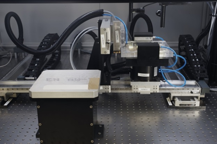
The IAI develops intra-layer integration processes for the printing of conductive tracks (Figure 1) as well as the mounting and contacting of discrete components on polymer substrates. In cooperation with partners within KIT institutes and external partners, different circuits (Figure 2) are being realized whereby both passive components, such as resistors and capacitors (IAM), and active elements, such as transistors (INT), are gradually replaced by printed components. For this Task the IAI is currently examining different printing and mounting methods with regard to suitability as an integration method.
 |
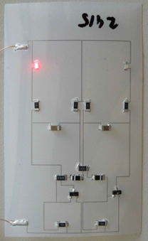 |
| Figure 1: Piezo ink jet print head for the printing of conductive tracks | Figure 2: Test circuit with conductive tracks printed on a polymer foil and mounted discrete components |
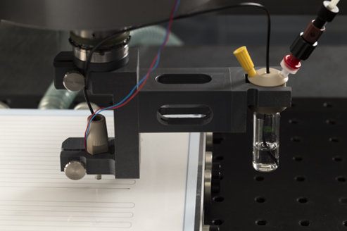
In terms of inter-layer integration, the IAI is examining different techniques for the precise alignment and joining of printed and stacked foil layers. This entails developing image processing, handling, dispensing, and laser-welding processes (in cooperation with IAM).
 |
|
Figure 3: Equipment for inter-layer integration of foils by aligned orientation via |